RTSystemDesign
Electronics for a laser measurement system
Project lead, electronics and enclosure design · 2013
A laser-research client needed custom electronics that could capture two brief light-detector pulses after every laser flash, compare them in real time, and fire a decision signal to the rest of its rig. The schedule was tight—with part of our fee riding on hitting the agreed delivery date—and the job required high-speed FPGA programming we did not have in-house.
I was upfront with the client about that gap and took full ownership of recruiting the specialist and delivering the complete box. While our FPGA contractor built the high-speed signal logic, I designed the interface electronics and enclosure, managed component sourcing and assembly, and led bench validation through on-time delivery.
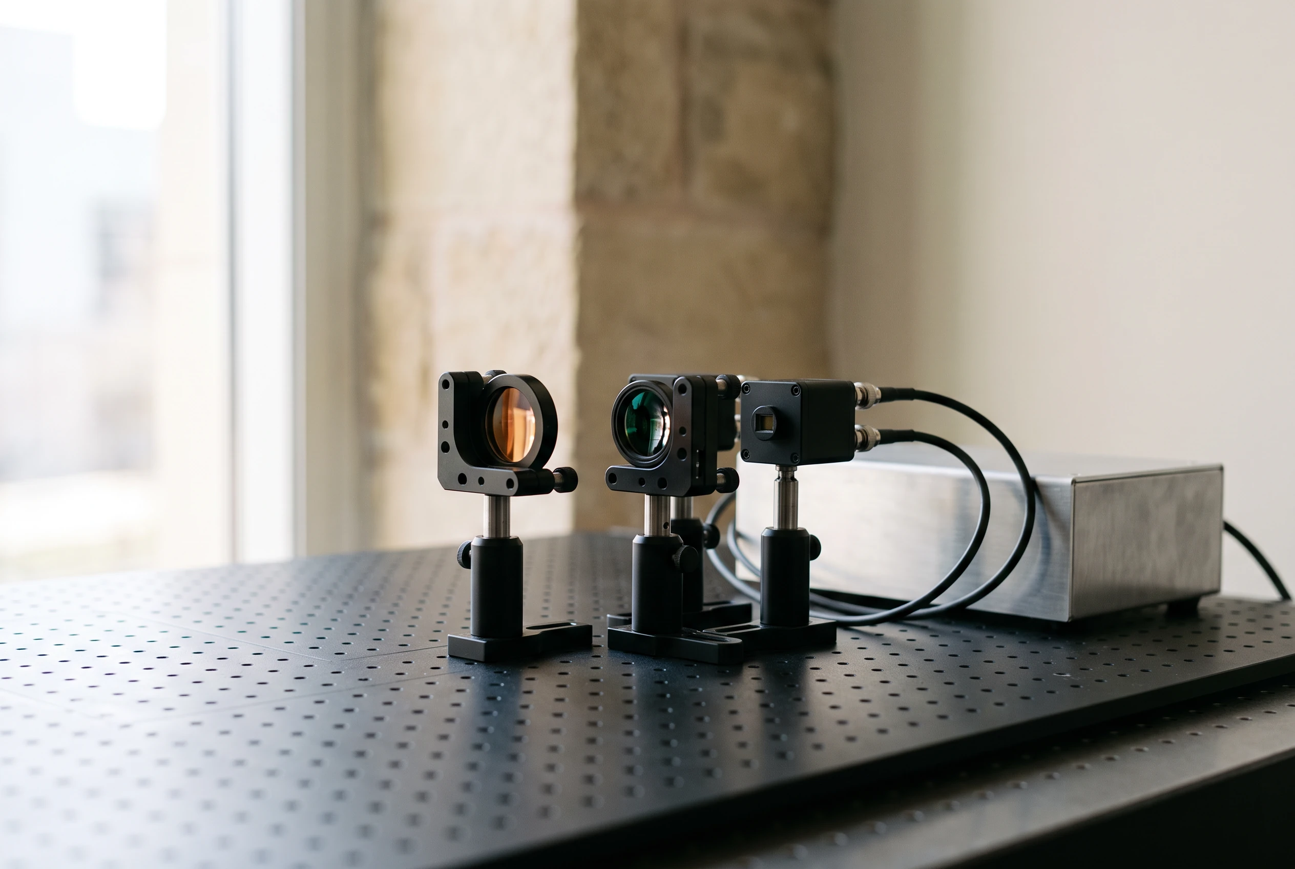 Enlarge imageEnlarge: Optical spectroscopy bench with mounted lenses and mirrors aligned toward dual photodetector housings and a custom brushed-aluminum electronics enclosure.
Choosing which part of the signal to measure
Right after a laser pulse fires, detector signals spike before settling into the brief decay window that actually carries useful experimental information. The electronics had to wait a precise delay after the trigger, sum both detector signals across the exact same narrow window, and compare their ratio against a chosen threshold.
Using an FPGA—a programmable chip built for deterministic, parallel signal processing—let the operator adjust both the trigger delay and integration window in five-nanosecond steps (five billionths of a second) to isolate the exact slice of the pulse that mattered.
Rather than forcing researchers to find stable timing settings by trial and error, we also built a calibration routine that swept across timing windows and measured how much the pulse-to-pulse ratio varied—highlighting settings that produced repeatable readings.
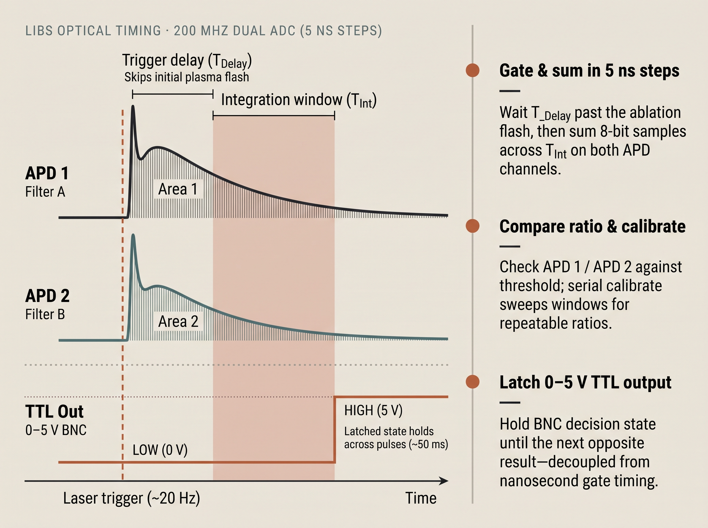 Enlarge imageEnlarge: LIBS optical timing logic showing 5-nanosecond dual-ADC gate delay, integration windows, ratio comparison, and latched 0–5 V TTL output.
Finding the specialist the project needed
With no time for a slow hiring search, I drove to UC San Diego and spent several hours walking through the engineering buildings looking for hands-on high-speed digital expertise. Spotting a research poster on FPGA architecture led me to the right specialist, and I put a cash retainer in place immediately to kick off the firmware work.
Being candid about what we had in-house—and hustling to close the gap fast—let us move immediately while I owned the surrounding hardware, interfaces, and client schedule.
Bringing the hardware together
To protect the deadline, we built around proven off-the-shelf FPGA and high-speed digitizer boards instead of waiting weeks to spin custom high-speed PCBs. I designed the custom interface circuitry tying those boards to the client’s detectors and downstream equipment, designed the enclosure, and ran purchasing and assembly.
Bridging the two sides of the experiment required careful timing design: the optical measurement happened in nanoseconds, whereas the client’s receiving equipment needed a longer, conditioned output pulse it could reliably detect. On the bench, we validated the complete signal chain independently of the client’s laser by feeding known electrical test pulses into the inputs across varying integration windows.
Giving the client control of the system
Hardware is only useful in a research lab if researchers can tune it as their experiments evolve. Alongside a clear quick-start guide, we delivered a straightforward computer interface where operators could adjust delay and window settings, set ratio thresholds, inspect live detector totals, and run the stability calibration routine.
We delivered the finished electronics package within the agreed September 2013 deadline and earned our full success fee.
Experience used here
Engineering project leadership · Electronics and enclosure design · FPGA specialist recruitment · High-speed signal processing · System integration · Supplier coordination · Client delivery